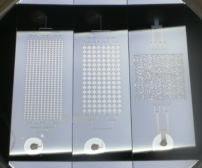
Wafer bonding is a technology that permanently joins two clean, atomically flat homogeneous or heterogeneous semiconductor substrates. After surface cleaning and activation, wafers are directly bonded under specific conditions via van der Waals force, molecular force and even atomic force. Bonding is a vital MEMS manufacturing step; optimal bonding processes guarantee mechanical stability, hermetic sealing and full device performance. Meiming Electronics has mature multiple bonding technologies to meet diverse client demands on substrate material, thickness, temperature and pressure.
Process Introduction
Wafer bonding is a technology that permanently joins two clean, atomically flat homogeneous or heterogeneous semiconductor substrates. After surface cleaning and activation, wafers are directly bonded under specific conditions via van der Waals force, molecular force and even atomic force. Bonding is a vital MEMS manufacturing step; optimal bonding processes guarantee mechanical stability, hermetic sealing and full device performance. Meiming Electronics has mature multiple bonding technologies to meet diverse client demands on substrate material, thickness, temperature and pressure.
Technical Applications
Bonding technology is extensively used in microelectronic device fabrication, including microcavity devices, cantilever devices, sacrificial layer formation and special microstructure manufacturing.
Process Capacity
Anodic Bonding
Eutectic Bonding (AuSn, CuSn, AuSi, etc.)
Adhesive Bonding (AZ4620, SU8, special bonding adhesives)
Wire Bonding
Multi-Layer Bonding
Silicon-to-Silicon Bonding
Flip Chip Bonding