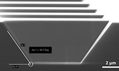
Etching is a selective removal technology for semiconductor substrate surfaces or surface thin films according to mask patterns or design specifications. It is an essential step in semiconductor and microelectronic IC manufacturing, serving as the core patterning process matched with photolithography. Etching is divided into dry etching and wet etching. Meiming Electronics has mastered various etching processes and will design cost-effective etching solutions with excellent performance based on customer requirements.
Process Introduction
Etching is a selective removal technology for semiconductor substrate surfaces or surface thin films according to mask patterns or design specifications. It is an essential step in semiconductor and microelectronic IC manufacturing, serving as the core patterning process matched with photolithography. Etching is divided into dry etching and wet etching. Meiming Electronics has mastered various etching processes and will design cost-effective etching solutions with excellent performance based on customer requirements.
Technical Applications
Etching technology is widely used in manufacturing semiconductor devices, integrated circuits, thin-film circuits, printed circuits and other micro-pattern structures.
Etching Materials
Silicon, silicon oxide, metals, quartz materials, etc.
Process Capacity
Available Etching Technologies: Ion Beam Etching (IBE), Deep Reactive Ion Etching (DRIE), Reactive Ion Etching (RIE), Focused Ion Beam (FIB) Etching, Inductively Coupled Plasma (ICP) Etching.